Page 91 - Electrician - TT (Volume 2)
P. 91
ELECTRICIAN - CITS


           IC7402 is a T.T.L NOR gate IC. It contains 4 NOR gates. For pin details, refer data book.
           NAND gate
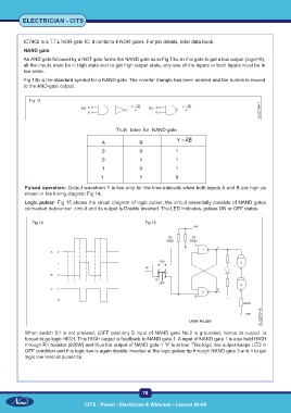
           An AND gate followed by a NOT gate forms the NAND gate as in Fig 13a. In this gate to get a low output (logic=0),
           all the inputs must be in high state and to get high output state, any one of the inputs or both inputs must be in
           low state.

           Fig 13b is the standard symbol for a NAND gate. The inverter triangle has been deleted and the bubble is moved
           to the AND-gate output.


             Fig 13


                                                 Truth  table  for  NAND gate

                                           A              B

                                           0              0              1
                                           0              1              1
                                           1              0              1
                                          1               1              0

           Pulsed operation: Output waveform Y is low only for the time intervals when both inputs A and B are high as
           shown in the timing diagram Fig 14.

           Logic pulser: Fig 15 shows the circuit diagram of logic pulser, the circuit essentially consists of NAND gates
           connected debouncer  circuit and its output is Double inverted. The LED indicates, pulses ON or OFF status.


              Fig 14                                        Fig 15


           When switch S1 is not pressed, (OFF position) B input of NAND gate No.2 is grounded, hence its output  is
           forced to go logic HIGH. This HIGH output is feedback to NAND gate 1, A input of NAND gate 1 is also held HIGH
           through R1 resistor (820W) and thus the output of NAND gate-1 'Y' is at low. This logic low output keeps LED in
           OFF condition and this logic low is again double inverted at the logic pulser tip through NAND gate 3 and 4 to get
           logic low level at pulser tip.


                                                           78

                                    CITS : Power - Electrician & Wireman - Lesson 60-69

