Page 138 - CITS - Electronic Mechanic - TT - 2024
P. 138
ELECTRONICS MECHANIC - CITS


           Through-Hole Plating: Conductive holes connect traces on both sides, allowing for more complex circuits.

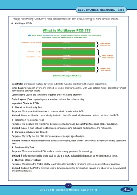
           4  Multilayer PCBs:


           Substrate: Consists of multiple layers of substrate material sandwiched between copper foils.
           Inner Layers: Copper layers are etched to create interconnections, with vias (plated holes) providing vertical
           connections between layers.
           Lamination: Layers are laminated together under heat and pressure.
           Outer Layers: Final copper layers are etched to form the outer circuitry.

           Important Tests for PCBs:
           1  Electrical Continuity Test:
           Purpose: To ensure that there are no open or short circuits in the PCB.

           Method: Use a multimetar  or continuity tester to check for continuity between desired points on the PCB.
           2  Insulation Resistance Test:
           Purpose: To measure the resistance between conductors and the substrate to ensure proper insulation.
           Method: Apply a high-voltage test between conductors and substrate and measure the resistance.
           3  Dimensional Accuracy Check:

           Purpose: To verify that the PCB dimensions meet design specifications.
           Method: Measure critical dimensions such as hole sizes, trace widths, and overall dimensions using calibrated
           tools.

           4  Solderability Test:
           Purpose: To ensure that the PCB surface is adequately prepared for soldering.
           Method: Perform solderability tests such as dip and look, solderability balance, or wetting balance tests.
           5  Thermal Stress Testing:

           Purpose: To assess the PCB’s ability to withstand temperature variations without delamination or damage.
           Method: Subject the PCB to thermal cycling between specified temperature ranges and observe for any physical
           or electrical failures.


                                                           123

                                    CITS : E & H - Electronics Mechanic - Lesson 73 - 76

