Page 74 - CITS - Electronic Mechanic - TT - 2024
P. 74
ELECTRONICS MECHANIC - CITS


           Output pin
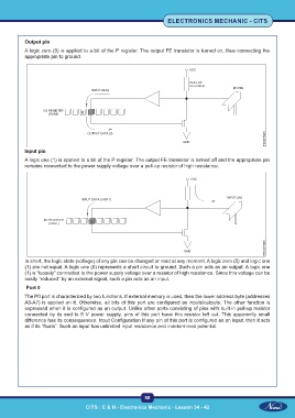
           A logic zero (0) is applied to a bit of the P register. The output FE transistor is turned on, thus connecting the
           appropriate pin to ground.


           Input pin
           A logic one (1) is applied to a bit of the P register. The output FE transistor is turned off and the appropriate pin
           remains connected to the power supply voltage over a pull-up resistor of high resistance.


           In short, the logic state (voltage) of any pin can be changed or read at any moment. A logic zero (0) and logic one
           (1) are not equal. A logic one (0) represents a short circuit to ground. Such a pin acts as an output. A logic one
           (1) is “loosely” connected to the power supply voltage over a resistor of high resistance. Since this voltage can be
           easily “reduced” by an external signal, such a pin acts as an input.

            Port 0
           The P0 port is characterized by two functions. If external memory is used, then the lower address byte (addresses
           A0-A7) is applied on it. Otherwise, all bits of this port are configured as inputs/outputs. The other function is
           expressed when it is configured as an output. Unlike other ports consisting of pins with built-in pull-up resistor
           connected by its end to 5 V power supply, pins of this port have this resistor left out. This apparently small
           difference has its consequences: Input Configuration If any pin of this port is configured as an input, then it acts
           as if its “floats”. Such an input has unlimited input resistance and indetermined potential.


                                                           59

                                    CITS : E & H - Electronics Mechanic - Lesson 34 - 42

