Page 19 - Electrician - TT (Volume 2)
P. 19
ELECTRICIAN - CITS


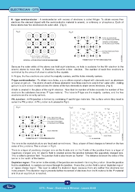
           N - type semiconductor : A semiconductor with excess of electrons is called N-type. To obtain excess free
           electrons the element doped with the semiconductor material is arsenic, or antimony or phosphorus. Each of
           these atoms has five electrons in its outer orbit.  (Fig 3)


               Fig 2                                          Fig 3


           Because the outer orbits of the atoms can hold eight electrons, no hole is available for the fifth electron in the
           arsenic atoms to move into.  It, therefore, becomes a free  electron.  The number of such free electrons is
           controlled by the amount of arsenic added to the crystals.
           In N-type, the free electrons are called the majority carriers, and the holes minority carriers.
           P-type semiconductor : To obtain more holes, a pure silicon crystal is doped with elements such as aluminum
           or boron or gallium.  The atoms of each of these elements have three electrons only in their outer orbit.  Adding
           gallium to pure silicon crystals allows the atoms of the two elements to share seven electrons. (Fig 4)
           A hole is created in the place of the eighth electron.  Now that the number of holes exceeds the number of free
           electrons the substance becomes ‘P’ type material.  The holes in P-type are the majority  carriers, and the free
           electrons are the minority carriers.

           PN Junction : A PN junction is formed by combining P and N type materials. The surface where they meet is
           called the PN junction. A PN junction is illustrated in Fig 5.

               Fig 4                                          Fig 5


           The ions in the crystal structure are fixed and cannot move.  Thus, a layer of fixed charges is formed on the two
           sides of the junctions. This is shown in Fig 6.
           There is a layer of positively charged ions on the N-side and on the P-side of the junction there is a layer of
           negatively charged ions. An electric field is created across the junction between the oppositely charged ions.
           This is called a junction field. The junction field is also known as ‘barrier’.  The distance between the sides of the
           barrier is the ‘width’ of the barrier.
           Depletion region : The carrier  in the vicinity of the junction are involved in forming the junction. Once the junction
           field is established, no carriers can move through the junction.  Hence the junction field is called ‘depletion region’
           or ‘space charge region’. This layer is called the depletion layer, because there are neither free electrons nor
           holes present. This depletion region prevents further movement of electrons from the N-material to the  P-material
           and thus an equilibrium is reached.


                                                            6

                                    CITS : Power - Electrician & Wireman - Lesson 60-69

