Page 61 - Electrician - TT (Volume 2)
P. 61
ELECTRICIAN - CITS


           Etching is done using any one of the following chemicals;
           –  Alkaline ammonia

           –  Sulpuric-hydrogen peroxide
           –  Ferric chloride
           –  Cupric chloride
           The ratio of ferric chloride and water decides the rate of etching. The typical ratio is, 100mg of concentrated ferric
           chloride powder/liquid for one litre of water. This Fecl3 is prepared in a plastic tray of suitable size such that the
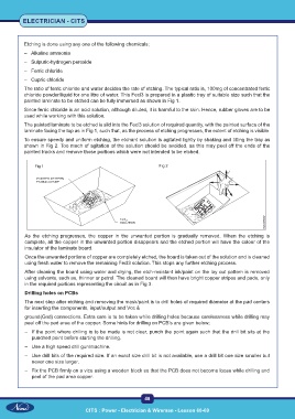
           painted laminate to be etched can be fully immersed as shown in Fig 1.

           Since ferric chloride is an acid solution, although diluted, it is harmful to the skin. Hence, rubber gloves are to be
           used while working with this solution.
           The painted laminate to be etched is slid into the Fecl3 solution of required quantity, with the painted surface of the
           laminate facing the top as in Fig 1, such that, as the process of etching progresses, the extent of etching is visible.
           To ensure speedy and uniform etching, the etchant solution is agitated lightly by shaking and tilting the tray as
           shown in Fig 2. Too much of agitation of the solution should be avoided, as this may peel off the ends of the
           painted tracks and remove those portions which were not intended to be etched.


               Fig 1                                             Fig 2


           As  the  etching  progresses,  the  copper  in  the  unwanted  portion  is  gradually  removed.  When  the  etching  is
           complete, all the copper in the unwanted portion disappears and the etched portion will have the colour of the
           insulator of the laminate board.

           Once the unwanted portions of copper are completely etched, the board is taken out of the solution and is cleaned
           using fresh water to remove the remaining Fecl3 solution. This stops any further etching process.
           After cleaning the board using water and drying, the etch-resistant ink/paint on the lay out pattern is removed
           using solvents, such as, thinner or petrol. The cleaned board will then have bright copper stripes and pads, only
           in the required portions representing the circuit as in Fig 3.

           Drilling holes on PCBs
           The next step after etching and removing the mask/paint is to drill holes of required diameter at the pad centers
           for inserting the components, input/output and Vcc &

           ground(Gnd) connections. Extra care is to be taken while drilling holes because carelessness while drilling may
           peel off the pad area of the copper. Some hints for drilling on PCB’s are given below;
           –  If the point where drilling is to be made is not clear, punch the point again such that the drill bit sits at the
              punched point before starting the drilling.
           –  Use a high speed drill gun/machine.
           –  Use drill bits of the required size. If an exact size drill bit is not available, use a drill bit one size smaller but
              never one size larger.
           –  Fix the PCB firmly on a vice using a wooden block so that the PCB does not become loose while drilling and
              peel of the pad area copper.


                                                           48

                                    CITS : Power - Electrician & Wireman - Lesson 60-69

