Page 65 - Electrician - TT (Volume 2)
P. 65
ELECTRICIAN - CITS


           Unlike in bipolar transistors in which the main current is both by electrons and holes, in contrast in FETs depending
           on the type(P or N type) the main current is either by electrons or by holes and never both. For this reason FETs
           are also known as Unipolar transistors or Unipolar device.
           There are a wide variety of FETs. In this lesson one of the fundamental types called as Junction Field Effect
           Trasistor (JFET) is discussed.
           Junction Field effect Transistor (JFET)
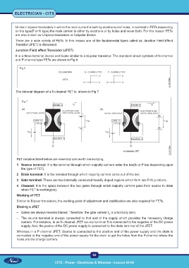
           It is a three terminal device and looks similar to a bi-polar transistor. The standard circuit symbols of N-channel
           and P-channel type FETs are shown in Fig 6.

              Fig 6


           The internal diagram of a N-channel FET is  shown in Fig 7.


               Fig 7


            FET notation listed below are essential and worth memorizing,
            1  Source terminal: It is the terminal through which majority carriers enter the bar(N or P bar depending upon
              the type of FET).

            2  Drain terminal: It is the terminal through which majority carriers come out of the bar.
            3  Gate terminal: These are two internally connected heavily doped regions which form two P-N junctions.
            4  Channel: It is the space between the two gates through which majority carriers pass from source to drain
              when FET is working(on).
            Working of FET
            Similar to Biploar transistors, the working point of adjustment and stabilization are also required for FETs.
            Biasing a JFET
            –  Gates are always reverse biased. Therefore  the gate current I  is practically zero.
                                                                     G
            –  The source terminal is always connected to that end of the supply which provides the necessary charge
              carriers. For instance, in an N-channel JFET source terminal S is connected to the negative of the DC power
              supply. And, the posive of the DC power supply is connected to the drain terminal of the JFET.
            Whereas in a P channel JFET, Source is connected to the positive end of the power supply and the drain is
            connected to the negative end of the power supply for the drain to get the holes from the P-channel where the
            holes are the charge carriers.


                                                           52

                                    CITS : Power - Electrician & Wireman - Lesson 60-69

