Page 66 - Electrician - TT (Volume 2)
P. 66
ELECTRICIAN - CITS


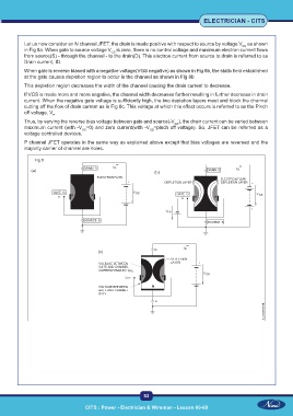
           Let us now consider an N channel JFET, the drain is made positive with respect to source by voltage V  as shown
                                                                                                   DS
           in Fig 8a. When gate to source voltage V  is zero, there is no control voltage and maximum electron current flows
                                              GS
           from source(S) - through the channel - to the drain(D). This electron current from source to drain is referred to as
           Drain current, ID.
           When gate is reverse biased with a negative voltage(VGS negative) as shown in Fig 8b, the static field established
           at the gate causes depletion region to occur in the channel as shown in Fig 8b.

           This depletion region decreases the width of the channel causing the drain current to decrease.
           If VGS is made more and more negative, the channel width decreases further resulting in further decrease in drain
           current. When the negative gate voltage is sufficiently high, the two depletion layers meet and block the channel
           cutting off the flow of drain current as in Fig 8c. This voltage at which this effect occurs is referred to as the Pinch
           off voltage, V .
                      P
           Thus, by varying the reverse bias voltage between gate and source(-V ), the drain current can be varied between
                                                                        GS
           maximum current (with -V =0) and zero current(with -V =pinch off voltage). So, JFET can be referred as a
                                                              GS
                                  GS
           voltage controlled devices.
           P channel JFET operates in the same way as explained above except that bias voltages are reversed and the
           majority carrier of channel are holes.

               Fig 8


                                                           53

                                    CITS : Power - Electrician & Wireman - Lesson 60-69

