Page 62 - Electrician - TT (Volume 2)
P. 62
ELECTRICIAN - CITS


           –  Ensure that all the points required are drilled because, once the components are mounted, drilling holes on
              the PCB may damage the mounted components due to vibration.

           After drilling holes, clean the PCB such that it is free from burr and dust. Apply varnish on the layout pattern, to
           protect the copper pattern from corrosion.
           Preparing and marking component lay out

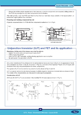
           A typical component side of a  PCB with the components marked on it is in Fig 4.

             Fig 3                                          Fig 4


            Unijunction transistor (UJT) and FET and its application


           Objectives: At the end of this lesson you shall be able to
           •  explain the construction and working principle of UJT
           •  make a quick test of UJT
           •  state the FET, JEFT principle, working biasing application as an amplifier
           •  list and explain the application of UJTs


           Unijunction transistor(UJT) is a three terminal semiconductor device as shown in fig 1a. In its appearance it looks
           like a transistor as shown in Fig 1b. As shown in Fig 1a, it consists of two layers(a P-layer and a N-layer) and
           therefore it has only one junction(hence its name, uni-junction).
           The symbol of UJT and its electrical equivalent circuit is shown in Fig 1c and 1d.
           UJT is a special semiconductor device because it exhibits negative resistance characteristics as shown in Fig 2.
           The details of the characteristics are discussed in subsequent paragraphs.
           Construction of UJT
           2646 and 2N 2647 UJT’s are available in the modified TO-18 case style as shown in Fig 1b.


               Fig 1                                          Fig 2


                                                           49

                                    CITS : Power - Electrician & Wireman - Lesson 60-69

