Page 75 - Electrician - TT (Volume 2)
P. 75
ELECTRICIAN - CITS


           Potentiometer R provides the facility for varying the intensity of light or speed of a universal motor.
                         4
           Snubber circuit: One problem with the Triac control is the sudden application of reverse voltage across the triac
           immediately after it has stopped conduction.  This is a serious problem when the load is a highly inductive as in
           motors. This reapplied voltage denoted by dv/dt can trigger-on (unwanted or false triggering) the device losing
           the phase control.
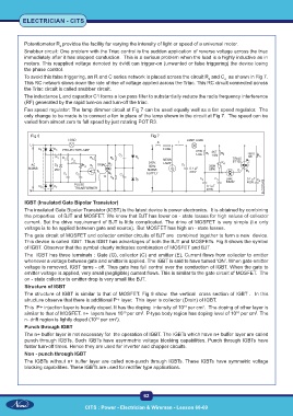
           To avoid this false triggering, an R and C series network is placed across the circuit R  and C   as shown in Fig 7.
                                                                                      4
                                                                                            4
           This RC network slows down the rate of rise of voltage applied across the Triac. This RC circuit connected across
           the Triac circuit is called snubber circuit.
           The inductance L and capacitor C1 forms a low pass filter to substantially reduce the radio frequency interference
           (RF) generated by the rapid turn-on and turn-off the triac.
           Fan speed regulator: The lamp dimmer circuit at Fig 7 can be used equally well as a fan speed regulator.  The
           only change to be made is to connect a fan in place of the lamp shown in the circuit at Fig 7.  The speed can be
           varied from almost zero to full speed by just rotating POT R3.


              Fig 6                                           Fig 7


           IGBT (Insulated Gate Bipolar Transistor)
           The insulated Gate Bipolar Transistor (IGBT) is the latest device is power electronics.  It is obtained by combining
           the properties  of BJT and MOSFET. We know that BJT has lower on - state losses for high values of collector
           current. But the drive requirement of BJT is little complicated. The drive of MOSFET is very simple (i.e only
           voltage is to be applied between gate and source).  But MOSFET has high on - state losses.
           The gate circuit of MOSFET and collector emitter circuits of BJT are  combined together to form a new  device.
           This device is called IGBT. Thus IGBT has advantages of both the BJT and MOSFETs. Fig 8 shows the symbol
           of IGBT. Observer that the symbol clearly indicates combination of MOSFET and BJT.
           The  IGBT has three terminals : Gate (G), collector (C) and emitter (E), Current flows from collector to emitter
           whenever a voltage between gate and emitter is applied. The IGBT is said to have turned 'ON'. When gate emitter
           voltage is removed, IGBT turns - off. Thus gate has full control over the conduction of IGBT. When the gate to
           emitter voltage is applied, very small (negligible) current flows. This is similar to the gate circuit of MOSFET.  The
           on - state collector to emitter drop is very small like BJT.
           Structure of IGBT
           The structure of IGBT is similar to that of MOSFET. Fig 9 show  the vertical  cross section of IGBT .  In this
           structure observe that there is additional P+ layer.  This layer is collector (Drain) of IGBT.
           This  P+ injection layer is heavily doped. It has the doping  intensity of 10 per cm .  The doping of other layer is
                                                                                   3
                                                                            19
           similar to that of MOSFET. n+  layers have 10 per cm . P-type body region has doping level of 10  per cm . The
                                                                                                         3
                                                   19
                                                                                                 16
                                                           3
           n- drift region is lightly doped (10  per cm ).
                                                3
                                        14
           Punch through IGBT
           The n+ buffer layer is not necessary for  the operation of IGBT. The IGBTs which have n+ buffer layer are called
           punch through IGBTs. Such IGBTs have asymmetric voltage blocking capabilities. Punch through IGBTs have
           faster turn-off times. Hence they are used for inverter and chopper circuits.
           Non - punch through IGBT
           The IGBTs without n+ buffer layer are called non-punch through IGBTs. These IGBTs have symmetric voltage
           blocking capabilities. These IGBTs are used for rectifier type applications.


                                                           62

                                    CITS : Power - Electrician & Wireman - Lesson 60-69

