Page 76 - Electrician - TT (Volume 2)
P. 76
ELECTRICIAN - CITS


              Fig 8                                      Fig 9


           Operation of IGBT
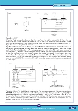
           When V  > V (threshold),  then the channel of electrons is formed beneath the gate as in Fig 10. These electrons
                  GS
                       GS
           attract  holes from p+ layer.  Hence, holes are injected from p+  layer into n-  drift region. Thus hole / electron current
           starts flowing from collector to emitter. When holes enter p-type body region, they attract more electrons  from n+
           layer. This action is exactly similar to MOSFET.
           Fig 11 shows the structure of IGBT showing how internal MOSFETs and transistors are formed. The MOSFET is
           formed  with input gate, emitter as source and n- drift  region as drain. The two transistors T  and T  are formed
                                                                                                  2
                                                                                            1
           as  in Fig 11.  The holes injected by the P+ injecting layer go to the n- drift region. This n- drift region is base of T
                                                                                                            1
           and collector of T .  The holes in the n- drift region further go to the p - type body region, which is connected to the
                          2
           emitter. The electrons from n+ region (which is emitter) pass through the transistor T2 and further in the n- drift
           region. Thus holes and electrons are injected in large amounts in n- drift region.  This reduces the resistance of
           the n- drift region.  This is called conductivity modulation of n- drift region.  Note that such conductivity modulation
           does not exist in MOSFET. The connection of T  and T  is such that  large amount of hole/electrons are injected
                                                           2
                                                     1
           in n- drift region.
               Fig 10                                       Fig 11


           The action of T  and T  is  like SCR which is regenerative.  The  gate serves as trigger for T  through internally formed
                                                                                       1
                             2
                        1
           MOSFET.  Fig 12 shows  the equivalent circuit.  In this figure observe that when gate is applied (V  > V (th)), the
                                                                                                GS
                                                                                                     GS
           internal equivalent MOSFET turns  on. This gives base drive to T . Hence T  starts conducting. The collector of T
                                                                             1
                                                                                                             1
                                                                    1
           is base of T .  Therefore T  also turns on. The collector of T  is base of T . Thus the regenerative loop begins and
                                                               2
                     2
                                  2
                                                                          1
           large number of carriers are injected in n- drift region. This reduces the on- state loss of the IGBT just like BJT.  This
           happens due to conductivity  modulation of n- drift region.
                                                           63
                                    CITS : Power - Electrician & Wireman - Lesson 60-69

